When you purchase through links on our website , we may pull in an affiliate commission . Here ’s how it works .
scientist have developed a new eccentric of razor - thin crystal motion picture semiconductor that enables electrons to move seven time faster than they do in traditional semiconductor — and it could have huge conditional relation for electronic devices .
In a study published July 1 in the journalMaterials Today Physics , physicist created an extremely lean film from a crystalline material call ternary tetradymite .
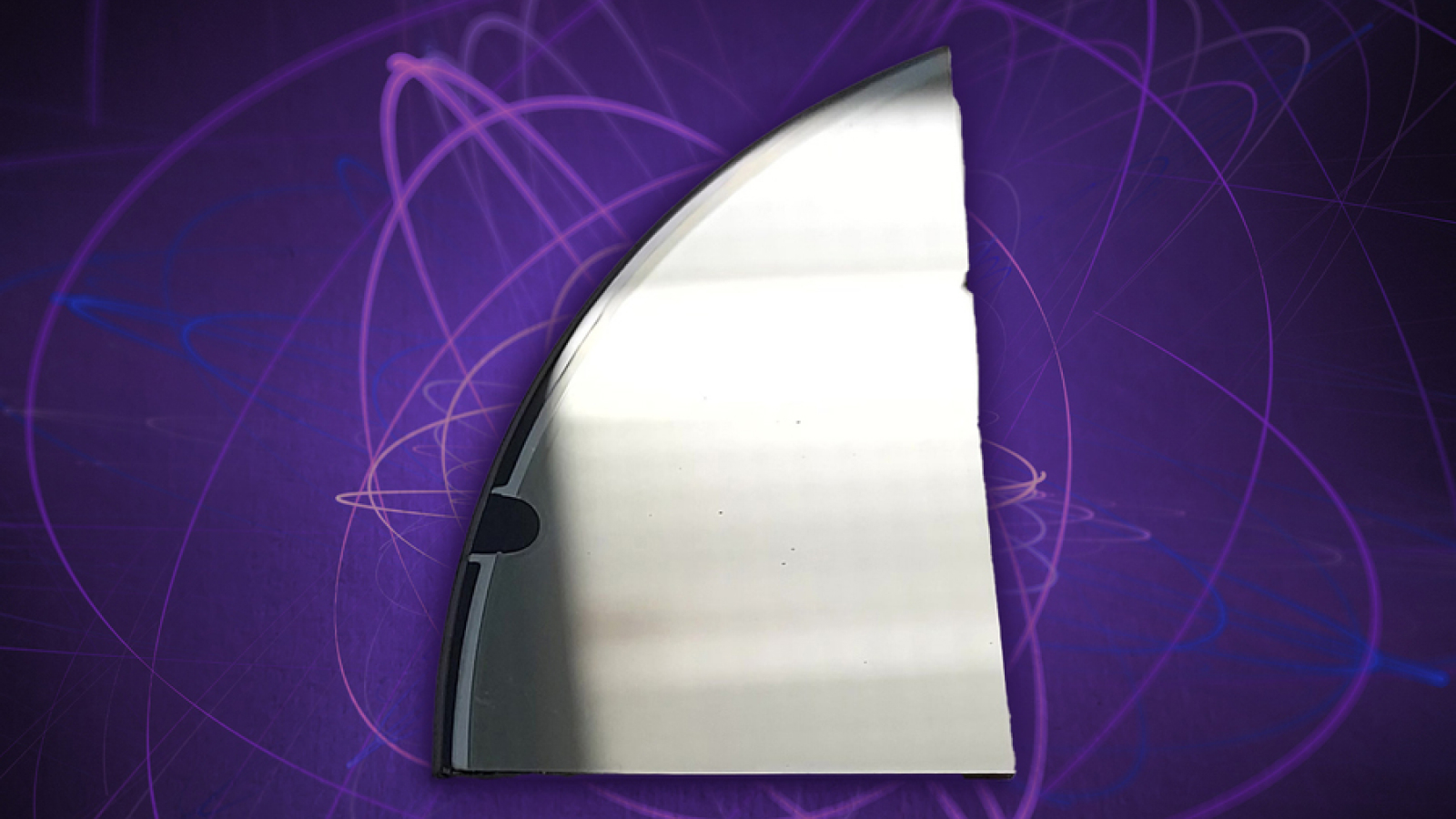
The new crystalline film is thinner than a human hair.
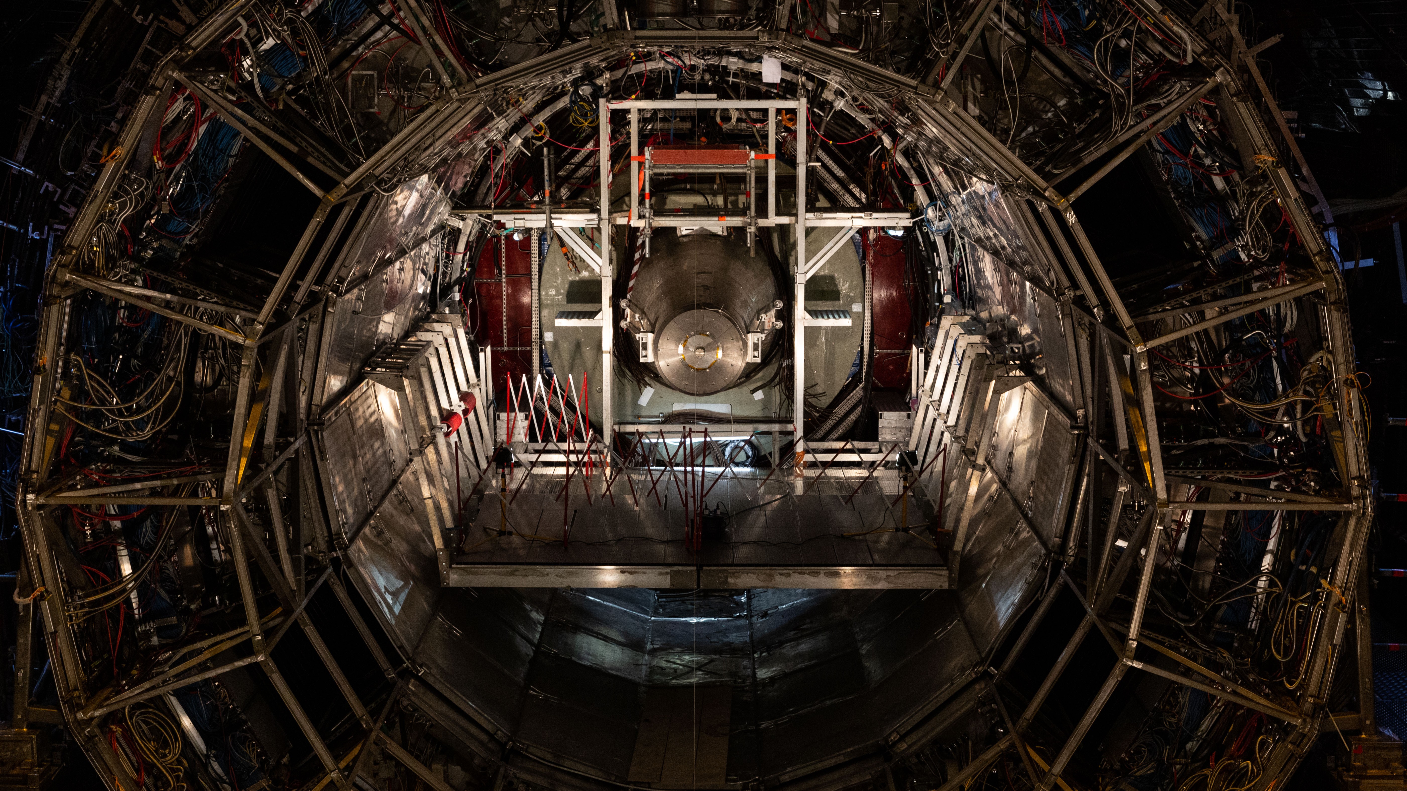
The photographic film — measuring just 100 millimicron blanket , or about one - thousandth of the heaviness of a human hair — was created through a process calledmolecular shaft of light epitaxy , which involves precisely controlling electron beam of molecules to build a material atom - by - atom . This outgrowth allow material to be constructed with minimal flaws or shortcoming , enabling greater electron mobility , a measuring stick of how easily electron move through a material under an galvanic field of operation .
When the scientist implement an electric current to the plastic film , they register electron moving at book - stop hurrying of 10,000 cm square per V - irregular ( cm^2 / V - s ) . By comparison , electron typically move at about 1,400 cm^2 / five - sin standard silicon semiconductors , and substantially slowerin traditional copper wiring .
Related : institutionalize next EVs could take indorsement with newfangled atomic number 11 - ion stamp battery tech
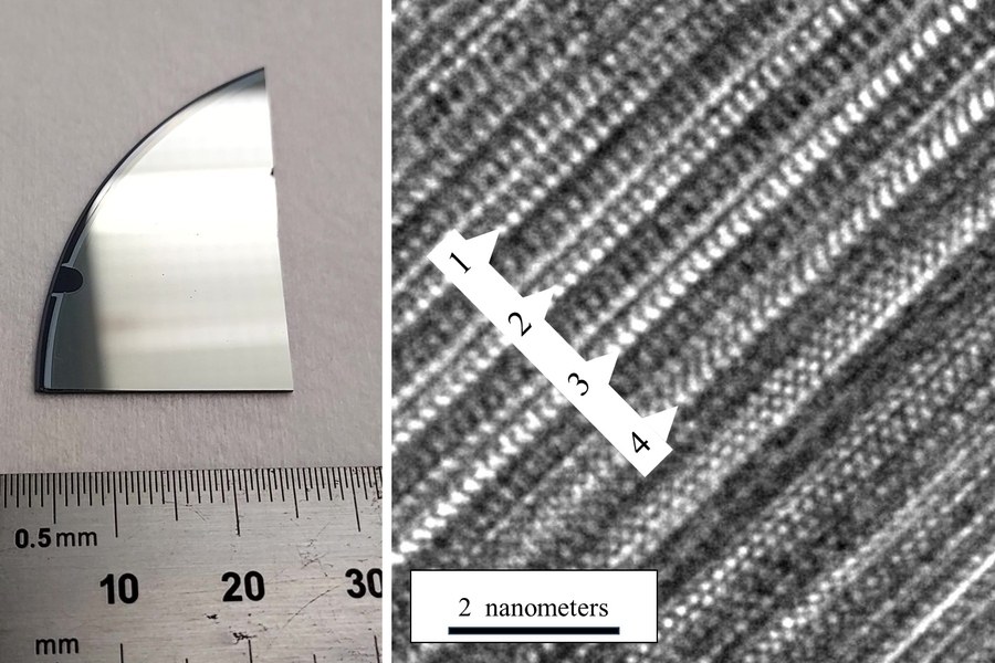
The thin film’s microscopic crystal structure, with minimized defects, allows electrons to flow through with high mobility.
This sky - high negatron mobility render to better conductivity . That , in round , paves the way for more efficient and powerful electronic gadget that give off less heat and lay waste to less vigour .
The research worker likened the film ’s belongings to " a main road without dealings , " enunciate that such materials " will be essential for more efficient and sustainable electronic devices that can do more work with less power . " Potential coating admit wearable thermoelectric devices that convert waste material estrus into electricity and " spintronic " devices , which employ electron twisting instead of charge to process information , the scientist said .
" Before , what people had reach in price of negatron mobility in these system of rules was like traffic on a road under construction — you ’re support up , you ca n’t drive , it ’s dusty , and it ’s a mess,“Jagadeesh Moodera , a physicist at MIT , said ina affirmation . " In this newly optimized material , it ’s like driving on the Mass Pike with no traffic . "
— China develop new light - free-base chiplet that could power contrived general intelligence operation — where AI is wise than humans
— Ultrafast optical maser - powered ' magnetic RAM ' is on the celestial horizon after raw breakthrough
— next electric railway car could go more than 600 miles on a single tutelage thanks to battery - boosting gel

The scientists measure electron mobility in the stuff by localize the pellucid flick in an passing insensate environment under a magnetised field . They then exceed electrical current through it and measuredquantum oscillations , which come about when electrical resistance fluctuates in reception to a magnetic field .
Even tiny defects in the stuff can affect electronic mobility by obstructing the movement of electrons . As such , the scientist hope that down the process for creating the film will produce even good results .
" This is show it ’s possible to go a giant stone’s throw further , when decent controlling these complex systems , " Moodera said . " This enjoin us we ’re in the right direction , and we have the right system of rules to proceed further , to keep hone this fabric down to even much thinner picture show and proximity mating for use in future spintronics and wearable thermoelectric gadget . "

China ’s ' 2D ' scrap could soon be used to make silicon - free chips
TSMC ’s upcoming 2 nm microchip is a breakthrough . Here ’s what it means for the futurity of tech — from AI to smartphones .
The constant surveillance of modern life could aggravate our learning ability function in ways we do n’t fully understand , disturb study indicate